Microstructured Optics for LED Applications
Optics for use with Light Emitting Diodes are described. Microstructured optics are available and customizable for a wide variety of applications. A few of these will be touched on. A methodology of designing these optics and the photometrics of the typical technology is overviewed.

.")


Introduction
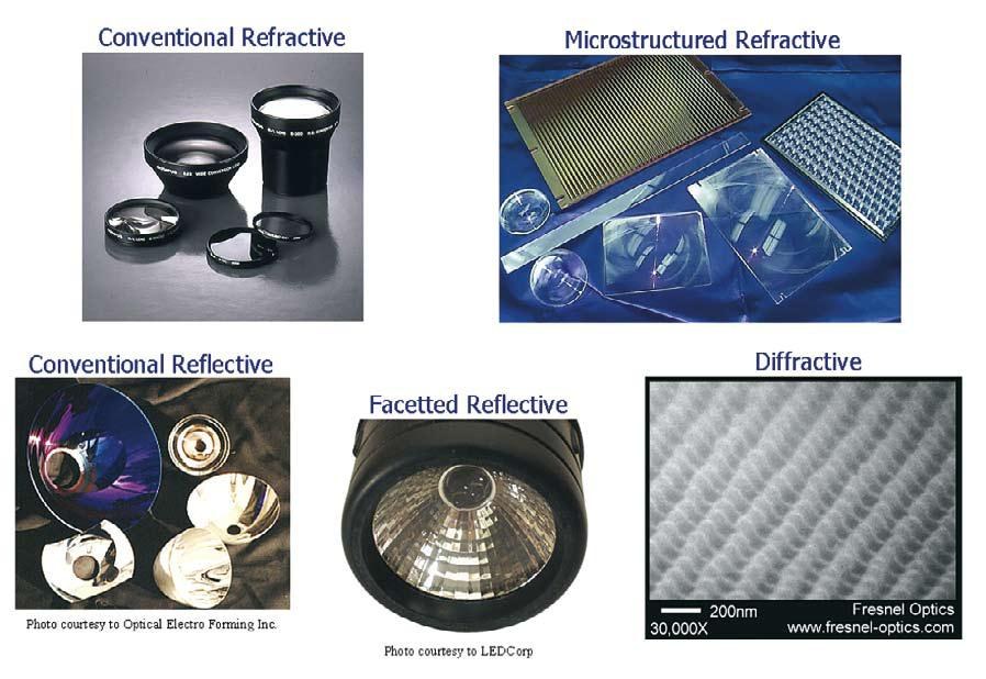
With the increasing popularity of LED’s in lighting applications, there is a need for engineered photometric control. Given exacting output requirements, it is unusual for a given supplier’s LED to produce the correct emission profile. This can be remedied with the use of auxiliary optics. Available classes of optics include refractive (continuous surface and microstructured), reflective (continuous and facetted) and diffractive. Examples are shown in Figure 1. This paper will concentrate on microprism refractive optics with some mention of reflectors.
The type of designs considered here are light energy directing designs or “nonimaging optics”. Some nonimaging design background will be outlined followed by mention of some specific LED commercial applications. Design methodologies for microstructured refractive optics will then be explored and a photometric analysis of a sample design will be presented. Finally a discussion on some salient issues regarding LEDs and microstructured optics is offered.
Background
Photometric plots
The required output specification is usually called out in photometric units: either Luminous intensity (lumens/steradian or lm/sr also known as candelas or cd) or Luminance (cd/m^2). Sometimes Illuminance (lm/m^2) is important (mostly for uniformity requirements).
Luminance is usually a calculated conversion from Luminous intensity (it can also be measured directly). Luminous intensity is a quantity commonly measured at photometric labs and a typical output from raytracing. The formula for converting from Luminous intensity to Luminance is:
where Lv is the Luminance, Iv is the Luminous Intensity, Avis is the visible area and θ is the Zenith Angle.
There are a variety of ways to represent the photometrics. Luminous intensity and Luminance can be represented on similar plot types. Useful representations are 3Dmesh, contour, polar, rectangular and Söllner.
3Dmesh is uncommon, but it can help as a method of visualizing what the photometric distribution is. It is done by plotting the Luminous intensity (or Luminance) magnitude in three dimensional coordinates. A 3Dmesh plot is shown in Figure 2 for a Luxeon LXHL-MW1A [1].
A contour plot is made by taking the hemisphere in which the light distribution emits and plotting the magnitude proportional to assigned colormap values on polar coordinates as shown in Figure 3. The rings of the plot are the zenith (or the angle from the polar axis) and the spokes are the azimuth (or the angle around the polar axis). See Figure 4 for the geometry of the coordinates.
When a specification is considered, (such as max allowed luminance outside of a given angular range), it is sometimes useful to assign a small number of discreet contour levels with the maximum magnitude being the limit for the first contour level. Then at the given zenith limit, the specification is easily observed by whether the first color level “bleeds across” the specification ring or not. For example, consider a specification that calls for less than 1000cd/m^2 outside of the 65° zenith angle. If the contour level from 0-1000cd/m^2 represents red, and >1000cd/m^2 is blue, on observing the plot, the spec is met as long as no red falls outside the region of the 65° zenith ring. This can be more informative than a polar plot which only takes several slices through the distribution, because the slices may “miss” a region where the specification is exceeded. This may not be an issue if the photometrics are strictly specified by the polar slices, but it is still useful to know if light is spilling out of the specified region.
A polar plot takes slices through a contour plot for constant azimuthal values. The polar axis on this plot then represents the zenith coordinate, and the radial axis is the photometric magnitude. Typically multiple slices are taken (for instance at 22.5 degree increments) with each slice overlaying the plot as a different color. An example is shown in Figure 5.
See Figure 5 (see LpR magazine)
The data from a polar plot can be equivalently plotted on rectangular axes. The x-axis is the zenith angle and the y-axis is the photometric magnitude. Again multiple slices can be overlaid with different colors as shown in Figure 6.
See Figure 6 (see LpR magazine)
The Sollner plot is another rectangular plot that is common for specifying office lighting. Its y-axis is instead the zenith angle and the x-axis is a logarithmic scale of the photometric magnitude. The angular range is typically truncated to the region of interest (instead of 0°-90° for example 45°-90°). This plot lends itself to quickly checking whether a maximum specified photometric magnitude is exceeded within a given angular range. See Figure 7.
See Figure 7 (see LpR magazine)
Finally, often the light distribution at a given plane is desired. This can be observed by setting a detector at the selected location and then collecting and plotting the flux per unit area there. This is an illuminance map (see Figure 8).
See Figure 8 (see LpR magazine)
A way to roughly simulate what the eye would perceive is to suppress the flux contribution of all rays that exceed a 10° observable cone. This is an approximation because the area of the flux distribution will usually be greater than the eye’s iris aperture. Furthermore, the foveal cone of the eye does not subtend an angle that large. It is typically necessary to consider at least a 10° cone however because reducing the angle, for example to 2°, greatly reduces the amount of rays in the flux distribution and produces a noisy illuminance map. Ideally however, visual simulation is achieved through a photorealistic renderer; see for example: Radiance[2] (which powers Adeline [3]), POV-Ray [4], Photopia [5] and Lightscape [6]. This topic is too vast to examine here, but it should be recognized that many rendering software packages exist and one needs to select a package that is sophisticated enough to import a source file representing the LED distribution.
Specifications
After generating the photometric analysis for a given design, the next task is to compare it to the requisite specification. Common lighting specifications include RP-1 [7] (for office lighting) and ITE [8] (for traffic signals).
The recommended preferred and maximum average luminances for office lighting are excerpted from Table 7-1 of Reference 7 and given below in Table 1. For comparing photometric data to RP-1, it is useful to overlay the specification boundaries on a Sollner plot of the data. To satisfy the specification, the data should not exceed the luminance boundary at the given angle (see Figure 9).
See Table 1 (see LpR magazine)
See Figure 9 (see LpR magazine)
The maintained minimum Luminous Intensity for LED traffic signals are excerpted from Table 1, section 4 of Reference 8 and reproduced in Table 2. To better grasp the numbers, a contour distribution can be created by bilinearly interpolating the table values into a large polar array. This is demonstrated for the red signal in Figure 10.
See Table 2 (see LpR magazine)
See Figure 10 (see LpR magazine)
For the purpose of a sample analysis an arbitrary specification is created. This distribution has a minimum peak intensity of 6.0candelas at six distinct propagation directions as shown in Figure 11. The specification shall require that the minimum luminous intensity exceed that of the distribution everywhere along the following polar slices: 22.5°, 45°, 67.5° and 90° (similar to an office lighting specification). In addition, it should exceed the distribution at every horizontal angle at the following declinations: 2.5°, 7.5°, 12.5° and 17.5° (similar to a traffic signal spec.).
See Figure 11 (see LpR magazine)
To compare the distributions, one can just look at the luminous intensities of the design and the specification side by side. But since the actual specification is called out in terms of polar and rectangular slices through the photometric distribution, it is most informative to instead slice both the data array and the specification distribution and then overlay the resulting plot lines on the same chart. The polar slice data comparison for the sample Luxeon LED is shown in the top row of Figure 12 and the rectangular slices in the bottom row. It is apparent that the specifications are not met. Auxiliary optics can be designed to shape the distribution to meet the specification. The design for an optical element to accomplish this will be consider in Section Design.
See Figure 12 (see LpR magazine)
Applications
Frontlighting and backlighting
Enormously popular applications of microstructured optics are in backlights and frontlights (see Figure 13). These are flat panel type waveguides used in LCD monitors, cell phones, pagers, PDAs, handheld games and other displays. Especially when using LEDs, fine photometric control of the light distribution is necessary in order to present the observer with a uniform observation field. This is usually accomplished with some form of waveguide preconditioning or integrating optic. This optic serves to illuminate the edge of the flat panel waveguide with a uniform input. Once inside this waveguide, microstructure is heavily relied upon. By either printed or etched dots or rows or patches of prisms, the light is selectively transferred out of the waveguide so that the whole panel appears uniformly illuminated. Still afterwards, more microstructure is important in providing the observer with the requisite screen brightness. Often a prism film is used to increase the gain and efficiency while recycling light that would otherwise be wasted.
See Figure 13 (see LpR magazine)
Traffic and rail signaling
A popular national trend is to replace incandescent traffic control signals with LED signals. There is a well defined standard for the luminous intensity performance of these signals (see ITE specification in Table 2 and Figure 10). Accordingly, any light that is directed upwards is a waste of power and can be redirected with the help of microstructured optics. Additionally, new designs with microstructured optics eliminate the unpleasant “discreetness” of large LED arrays by using higher intensity modules in a rear projection fashion (a example is shown in Figure 14). Custom lens elements implementing microstructured optics are ideal for redirecting these sources to a pleasantly uniform ITE specification.
A similar application is in the Rail signal industry. Rail signals are different from traffic signals in that they are mostly viewed in-plane (instead of significantly declined from the optical axis). They also have the unique requirement of being visible from far away and all throughout the subtended range a train operator perceives while traveling past the signal. Additionally, it is undesirable for train operators on the opposite side of the sign to have visibility of the light (light directed in this region is also wasted energy). Consequently a well engineered “side lobe” is required. The use of microstructured lenses and prism arrays makes all this possible.
See Figure 14 (see LpR magazine)
Flashlights
In an LED flashlight application, multiple LEDs may be used as the light source. This array is larger than a single typical flashlight bulb and for that reason it may be too unwieldy to create an effective reflector. Light collection and collimation can be improved by using a Fresnel lens on the output of the flashlight instead.
Office lighting
Although the author currently does not know of any office lighting fixture yet that implements LEDs, it is probably not unreasonable given the current state of the technology to design an RP-1 compliant direct/ indirect fluorescent/LED hybrid. The downlight requirements for direct/ indirect illumination are not extreme so using optically conditioned high intensity LEDs is plausible. At the same time, all uplight contributions can be provided by the fluorescent (instead of splitting it between uplight and downlight) so a fixture that normally uses two fluorescents may potentially be replaced by a fixture that uses a single fluorescent in combination with LEDs. The color rendering of such a hybrid however may be unusual.
Video Projection
Potential for microstructured optics may yet exist in video projection with the advent of newer LEDs. Traditionally plastic optics cannot be applied as source conditioners (i.e. field lenses and lens arrays) because the close proximity of the plastic to the extremely high temperatures of the incandescent source damages the optics. It would be highly desirable to use plastic optics in this application over glass because of plastic’s lightweight. Should LED brightness become sufficient for video projector applications, their inherent high efficiency and low thermal output (when compared to a comparable incandescent source) could make the use of plastic optics for lamp conditioning much more reasonable.
Additionally, there is the option of molding in a Moth-eye structure [9] for improved efficiency. Aside from the incremental tooling cost, process cycle time and manufacturing unit cost are marginally increased compared to a similar part without Moth-eye. In comparison to thin film coatings, the performance and value is enhanced considerably [10].
Miscellaneous
Of course the potential applications for LEDs are innumerable. For any of those applications where fine photometric control is required, or simply a different distribution from the manufacturer supplied LED is preferred, microstructured optics may be used in conjunction. More examples would include sign illumination in which optics can more evenly distribute the bright LED spots over the face of the sign, artistic lighting in hallways, movie theatres and galleries, marker lighting for roads and runways in which a cylindrical upward inclined distribution is desired, machine vision, automatic teller bank machines, pedestrian signs, automotive interiors such as for the instrument panels and for the dome lights, automotive exteriors such as for the brake and signal lights, street lighting, ring lights etc.
Design
A concise description of Illumination System design is given in Reference 11. To summarize, the process involves: building the fixed geometry, accurately modeling the source, determining the requirements, evaluating simple initial concepts, optimizing a selected concept, verifying the performance given geometric deviations, tolerancing, prototyping and finally testing [11]. The sample design presented in this section loosely follows these tenants. No geometric deviation or tolerancing is performed however and as of this writing the photometrics for the sample design presented have not yet been verified by testing.
Optical modeling tools
There are numerous ways to create a model of an optical layout. Tools of the trade commonly consist of a mechanical CAD package, a sequential raytrace package with global optimization, a non-sequential raytrace package and radiometry ray generation software.
One of the most straightforward ways of setting up a layout for raytracing is to draw the setup in a mechanical CAD package (SolidWorks [12], ProEngineer [13], Rhinoceros [14], AutoCAD [15] to name just several). Once completed most CAD programs can export to a format that can be imported by most raytrace packages. This methodology can be tedious for design optimization because each decided change in geometry requires redrawing the system, re-exporting it from the CAD package and re-importing it to the raytrace software. The process can be streamlined somewhat by using parametric software such as SolidWorks or ProEngineer. Parametric CAD software defines its geometry according to variable constraints. By judiciously constraining the model, the entire geometry can be quickly regenerated just by changing the value of a variable.
Sequential raytrace packages excel at quickly raytracing and optimizing an optical layout. The great speed of the software comes from the assumption that light will always travel to incidence on the next optical surface defined in the database. This is perfectly acceptable for imaging systems. Also adding to the power of most sequential raytrace software is the inclusion of global optimization algorithms in the software. By defining a figure of merit (such as spot size) and some system variables (such as radii of curvature), the global optimization routines can modify the system automatically until optimum performance is achieved. Popular software in this category is OSLO [16], Zemax [17] and CodeV [18].
For nonimaging systems and for stray light analysis of imaging systems, where light does not necessarily travel sequentially, a non-sequential raytrace package is required. In a non-sequential raytrace, light is permitted to reverse direction and become incident on optics it has already traversed, it can get trapped between surfaces, or it can skip the next optic in sequence altogether. Because of this generality, nonsequential raytracers trace rays much slower. This tends to make automatic global optimization more difficult to implement. Popular software in this category is ASAP [19], TracePro [16] and LightTools [18]. ASAP has a linear optimizer built in which can be readily applied in the design process. TracePro and LightTools have none, but the underlying macro languages are substantial enough to write one from scratch.
In order for a raytrace simulation to be as close to reality as possible, it is best to have the actual source photometrically characterized. This can be done by accurately measuring the source in a photometric lab. A typical photometric report will include the photometrically accurate far field luminous intensity values. From this data, careful calculation can result in the definition of a source model that is approximately apodized in accordance with the real source. It is most convenient however to use a software package such as ProSource [20] coupled with photometric measurements supplied by Radiant Imaging [20]. This allows the designer to generate accurate ray distributions via a nice user interface.
Other useful software includes scientific data visualization software (IDL [21], PV-Wave [22], Origin [23]) and capable programming languages (C/C++, Perl, Fortran and many others). Data visualization is an important tool in combination with raytrace packages because the data analysis portions of raytrace software are comparatively limited for purposes of calculation and publication. Programming language functionality adds similar capability, and also can be used to augment the raytracing software functionality.
Choosing an LED
Often, a customer seeking a tailored photometric output will already have an LED specified. It is most convenient for the designer if the LED is common enough to have been characterized and published in the Radiant Imaging Source database [20]. Any and all photometric data that can be supplied is useful in the design. It is also appreciated when a supplier of LEDs has gone through the effort of characterizing their LED sources and provide the data as requested.
If the design engineer has the liberty to choose an LED from the start, a significant factor in choosing a supplier is the free availability of characterization data (for example, downloadable photometric characteristics and published mechanical CAD drawings). This reduces the initial steps of acquiring varied samples of LED’s for measuring their characteristics. With photometric data readily available, a design feasibility study, (and indeed a full design) can be completed without having to receive a physical sample.
LED source modeling
Before considering how to shape the design photometrics with optics, it is paramount that an excellent source representation be used. Approximations and inaccuracies will at best transfer linearly through the system effecting error in the results. More likely though, errors will be compounded through the ray propagation yielding extra unrealistic results and incorrect flux magnitudes. (Concerning source modeling, see for example, References: 24, 25, 26 and 27.).
The LED source model can be simulated either by geometric detail or by ray generation based on accurate photometric measurements of the LED [24, 27]. Raytraces based on a characterized source model generally produce photometrics that are more accurate than a strictly geometric source model. However, if the source is to be used in a system where light may be recycled and impinge back on itself, it is essential to have its geometry included. The following merges the CAD geometry for a Luxeon 1-Watt white LED (LXHL-MW1A) [1] with the Radiant Imaging generated rayfile for this LED.
Figure 15 shows several views of the CAD geometry for the LED with the rayspots overlaid. The origin for both the CAD and the ray representations are coincident and is located at the center where the glass envelope meets the base. ProSource creates rays at arbitrary starting positions. As shown in Figure 15 all of the rayspots originate inside the boundary definitions of the LED. If the LED geometry is to be included in the raytrace, this is not where the initial ray coordinates belong. ProSource generates the rays from the perspective of an observation plane after the rays have already left the LED. Putting the rays back behind the glass dome and propagating them through again is not correct. To get the rays “out” then, they should be free-space propagated to an exterior dummy surface. This is accomplished with an absorbing shell located to surround the transmissive portion of the LED (Figure 16). The LED geometry is removed, and the rays are inserted (Figure 17).
See Figure 15 (see LpR magazine)
See Figure 16 (see LpR magazine)
See Figure 17 (see LpR magazine)
Next the rays are propagated (through free space) to be absorbed at the shell as shown in Figure 17. Note that some spurious rays are not coincident on the shell. In reality, this is not plausible because all emitted light should only come through the transmissive window of the LED. Most likely this is caused by ProSource reconstructing ambient scattered light. These rays are a small fraction of the total flux (less than 0.5%) and are deliberately dropped and ignored in further raytraces. The rays that are captured at the shell are transferred to a new rayfile to be used for all future raytraces. The CAD geometry for the LED is added back in and the location of the rays are plotted in Figure 18.
See Figure 18 (see LpR magazine)
Reflector design
The science of designing a reflector to maximally concentrate light from a source emitter is well researched (many useful publications are compiled in Reference 28). One type of reflector which can maximally redirect light output from an input plane is called a Compound Parabolic Concentrator or CPC [29, 30, 31, 32].
A schematic of a CPC is shown in Figure 19. As per the variables defined in that Figure, the following are some useful formulae for CPC design [29, 30]:
By choosing a smaller value for θmax, a higher degree of collimation is achieved. However, this also very quickly increases the requisite length (L) of the CPC. This can be traded off with not extending the CPC length out to L. Hinterberger [29] notes that truncating the reflector at 2/3L does not decrease the aperture diameter very much. Although, in his application, the CPC is used to collect light onto the focal plane (instead of collimating a source placed at the focal plane). When truncating the CPC length for source collimation, careful attention should be paid to its effect on the output half-angle.
See Figure 19 (see LpR magazine)
It can be shown that if a CPC reflector is converted into a solid dielectric with an index of refraction n satisfying: 2 ≥ n ≥ √2 (a range of indices covered by common materials) then total internal reflection is supported at the CPC walls.� This method can have significant cost benefit by eliminating the need to add a reflective coat. Furthermore, an engineered microstructured surface can be incorporated into the output surface for additional photometric control. In this way, both the light collector and a refractive control structure can be formed by a single injection mold.
At least one company capable of supplying CPC reflectors on a custom manufactured basis is Opti-Forms [33].
Refractive microstructure design
• Layout
The approach taken for designing a refractive microstructure is highly dependant on the application. For designing and manufacturing components in a well developed field, the design can practically be automated and therefore completed at little to no cost. An example is the design of a collimating Fresnel Lens. Since generalized software has been written to create facet geometry according to a lens prescription, the lens design is practically a commodity. The most significant costs are for tooling and manufacturing.
A stringently specified project will be much more complex. As an example, take the arbitrary specification fabricated in Section Specifications, Figure 11. Accordingly, the intent of this section shall be to take the on axis output from the LXHL-MW1A seated in the CPC and create six radiating off axis spokes. To begin, it is necessary to choose an optical structure of approximate proper form. This will give the optimization process its necessary starting point. In this case we will select a six-sided pyramidal structure; each facet of the pyramid will direct light toward one of the spoke directions [34].
Early in the design process, it is substantially important to consider tooling and manufacturing. Given the unlimited design flexibility within the scope of design software, it is easy to create a design that cannot be tooled or is prohibitively expensive to manufacture. It is frustrating to put significant effort in developing an optimal design to only later find out that it cannot be made. Sometimes it is possible to alter the design to make the part realizable, but it will inevitably be at the cost of performance. Usually it is best to include tooling and manufacturing constraints within the optimization process.
Depending on the tooling process used, different constraints may exist. In this case, the tooling is made by diamond ruling. We can form a six sided pyramidal structure by engraving crosscuts inclined to each other by 60° (see Figure 20). This will not create standalone pyramids; subprism features will also be formed. Understanding these features and including them in the design process is essential. To accomplish this, it is useful to make a three-dimensional representation of the solid geometry in CAD software (see Figure 20).
See Figure 20 (see LpR magazine)
On considering pitch, it is usually not so important to design the microstructure to the exact dimensions of the finished product. When the far field luminous intensity distribution is the specification of concern, often 10 prisms will do almost as good a job as 1000. The requirements are that the facet angles be maintained and the ratio of geometry feature dimensions remain fixed. The size of the microprisms can usually be chosen to satisfy the aesthetic requirements (whether the features should be visible to the unaided eye or not). Also tooling may be considered in selecting the pitch. Larger feature sizes decrease the time it takes to make the tooling master. Especially fine structure can approach the limit of tooling capability in addition to degrading performance as the ratio of feature size to tooling error (burrs, radiused edges etc.) decreases.
Furthermore, it is beneficial to exploit large facet size in the computer model itself. Generating numerous quantities of prisms in the model requires the computer simulation to solve a plethora of ray-boundary intersections. This is time consuming even on the currently fastest available computer hardware. Design iterations can proceed much more efficiently if larger size prisms are considered. An additional trick which can reduce the number of prisms stored in the raytrace database is to generate only several rows of prisms and then to bound them on either side by perfectly reflecting mirror planes. It is important that the planes be located such that symmetry of the facet structure is preserved (that is, in unfolding the prisms about the mirror planes, the microstructure should appear uninterrupted). This technique is not always possible and it is inaccurate at the boundaries, but for design purposes, it saves a lot of time. After design is complete, or during the last few iterations, the pitch may be reduced to actual size and the full volume of prisms generated (removing the perfect mirror planes) to verify the photometrics. This may not always be possible however when particularly small prisms are applied over a very large area; such great numbers of geometric definitions may exceed the capabilities of the software or take eons to raytrace.
With some of the new features being implemented in raytrace software, the issue of pitch and number of prisms affecting raytrace time can become mute. If the prism structure is simple enough, the virtual microstructure ability of RepTile in TracePro [16] and 3D‑Textures in LightTools [18] can apply vast numbers of prisms to a surface with the definition of a single facet period.
• Optimization
Once a the basic geometric form is developed, a process of optimization may commence. This can range anywhere from completely manual to nearly fully automated. In a manual optimization, each iteration would involve regenerating or reprogramming the facet geometry based on intuition and on how previous designs performed. With moderately stringent photometric specifications, and a solid grasp on how the optical facets interact with the light input, a manual optimization is completely reasonable and may be the quickest way to achieve a final design.
If after experimenting with a few manual optimization iterations, it becomes apparent that too many factors are interacting to seek a resolution by hand, then an automated optimizer should be applied. This is much more time consuming to set up initially, but it is far more efficient at characterizing large numbers of possible geometries then a manual process.
The first step in automated optimization is to define an error function (or figure of merit). The error function is some way of quantitatively defining how good the system performance is with a single number. As the error function approaches zero, the system performance improves. The design of an appropriate function can be complex. In this case, and in many other cases where just the luminous intensity distribution is of concern, it can be simple. The error function can be defined as the difference between the total flux of the LED and the amount of flux contained within the desired propagation spokes. If all flux was contained within the spokes, then the error function would be zero and an optimum design would be signified. In this example, there is no restriction on cutoff angle, but if a specification were to call for an explicit cutoff, an additional factor should be added to the error function to strongly punish the system merit until the cutoff requirement is satisfied.
The next step is to figure out what parameters of the system may be allowed to vary in order that an optimal geometry will be obtained. Typical parameters are facet slope angles, draft incline angles and pitch to height ratios. To follow, much geometric calculation must be done to fully define the geometry based on these parameters. Care must be taken to neither over-constrain nor under-constrain the geometric definitions. With each optimization loop, the geometric definitions will be referenced procedurally. The procedure call will only provide the designated parameter variables from which the entire geometric representation must be created. It is also useful to include some reality checking functionality to weight the algorithm against driving the system towards a physically unrealizable geometry.
Before hitting the “go” button, there will be a number of remaining details to wrap up depending on the application. Of course the underlying flow control of the optimization process must be implemented. Some software includes built-in optimization routines. For others, it may be necessary (or preferable) to write one from scratch (some of the common software available is briefly discussed in Section Optical modeling tools). Also, optimization time should be considered. A balance must be struck between accuracy and iteration time by deftly manipulating the following parameters:
• number of rays to trace
• ray splitting and/or ray scattering
• ray termination
• geometric sampling resolution
• feature periodicity (when not using virtual microstructure)
If all goes well, then a solution may be found. Keeping track of all the geometries and the results of their merit function is paramount when a large number of iterations are traversed since the terminating solution (or more likely, the current solution being analyzed when you hit the “cancel” button) may not be the best system. This may be accomplished with supplementary software or scripting programs designed to analyze the wealth of raytrace output files and compile the results into a convenient table. The table should include enough information to recreate the system. It is also convenient to sort the results in terms of the error function and to include other analytical numbers such as output flux, efficiency and so forth.
If an acceptable solution is not found, the optimization process starts over again. This can include anything from redefining the original geometry paradigm, to providing more (or less or different) degrees of freedom in the way the algorithm modifies the geometry or to simply altering the initial conditions of optimization.
Results
The photometric results are analyzed as described in Section Photometric plots (see Figure 21). These results are compared to the specification of Figure 11 as described in Section Specifications (see Figure 22). The photometric requirements exceed the specified minimum values at all angles and therefore satisfy the specification.
The predominant feature of generating six off axis “spokes” is achieved. As shown in Figure 21 however, there is an added on-axis lobe to the distribution. This lobe is not strictly forbidden by our specification. As such, it should not be a problem. Admittedly though, it is a source of inefficiency, robbing light from the specified lobes. Also, although the on axis lobe may not be prohibited in a customer’s original specification, a dialog must be opened to communicate the feature and prevent surprise. Without having realized it before, the customer may find that some photometric quirks actually are unacceptable and should be added to the specification. Still, given time and cost constraints it must be decided if any such peculiar photometric incarnations are acceptable. This also needs to be balanced in conjunction with the realization that further complicated design may yield microstructure features that prohibitively increase the tooling cost.
See Figure 21 (see LpR magazine)
See Figure 22 (see LpR magazine)
Discussion
LED vs. fluorescent
In designing microstructured optics for traditional lighting applications that use fluorescent sources, most of the methodology previously discussed for LEDs is directly applicable. A typical difference is the wide availability of photometric characterization for LEDs, which are highly accurate. Whereas such characterization files for fluorescent lamps are not freely published and are more expensive to generate. Thereby it is more common to use a less accurate geometrical model for fluorescent lamps. Furthermore, the emission cone of an LED is much more well confined then a cylindrical tube. This makes it easier to control the output distribution at a high efficiency since the LEDs can be spaced such that there is no or minimal overlap of the light distribution on the optic between neighboring sources. Conversely, this makes achieving a visual uniform field more difficult.
Source obscuration
The non-uniform illuminance pattern of the LED near field causes the significant complaint of source visibility. This generally occurs in applications where an LED is closely spaced to an optic. On the other side of this optic is the requirement for no source visibility with highly uniform illumination. This is a fairly tall order. Commonly, a high angle diffuser is used. A chief problem is that with said diffuser placed closely to an LED, its near field illuminance pattern is projected onto the diffuser and is consequently immediately visible and objectionable. A standard solution is to space the source as far away from the output optic as possible and use multiple diffusive layers maximally spaced. This is typically unwanted because it uses a large volume and is inefficient.
Under the constraints of small LED to lens distances, the solution to uniform output lies in light recycling. Injecting the LED source distribution into a tailored waveguide can be used to pre-condition the light into a uniform field. Waveguide extraction however can be an inefficient process. Some solutions to this problem are currently being investigated at Reflexite Display Optics with a strategic partnership for manufacturing technology that is much more highly efficient and can effectively obscure the source over a short distance.
Rigorous design vs. “plug and play”
The rigorous computer design method set forth is the recommend design paradigm, however, it is still quite popular to design with the “plug and play” approach. That is, buy some LEDs, maybe grab a lens, install it in the system, turn it on and see if it works. For loosely defined photometric requirements, indeed this might be the preferred design method because it is cheap and fast. If during the course of “plug and play” design one finds that trying multitudes of LEDs with random optics just is not working, a custom design would probably help. It may even be preferred to seek a customized design even when a plug and play solution is available; due to the precise photometric control that can be exercised with a microstructured optic, a photometric output may be sought that directs all light where it needs to go with very little stray energy outside of the requisite minima. This ensures maximal light utilization and promotes power conservation.
Inter-Compatibility
For any project in which an LED source is to be used, the designer should also take into concern obsolescence. As manufacturers refine their LEDs, it is not always a simple matter to unplug the old model and “drop in” a new one. For example, given that the trend is to increase brightness, for specifications that indicate a maximum luminance for a given cutoff angle, dropping in a brighter LED may exceed acceptable cutoff. Also, for a tightly toleranced layout in which the emission profile of the LED is precisely controlled, dropping in a new LED would be flawed if the new LED had a slightly different emission profile. For this reason, it is preferable that LED manufacturers carefully maintain LED emission profiles to be constant through LED generations.
At the discretion of the engineer based on the project requirements, system dependence to a specific LED can be minimized by loosening up the tolerances (usually at the expense of some system performance). Then when a new LED is installed it may be possible to bring it into specified performance by slightly adjusting the optic to LED distance. That is to say, adjustment of the emission profile may be tweaked by “focusing” the lens to different locations based on the LED. Allowing for such mechanical adjustments has the added benefit for optics that might be used simultaneously for several different color LEDs or several different manufacturer’s LEDs (or both). Each unique LED may have a distinct “source to optic” distance. The final output profile for each optic however can be very similar. The alternative is to change the optical element surface structure per LED type. Each LED type would require its own redesigned optic and new molding tools would have to be made. Additional molding tools would have to be made later as newer generation LEDs replaced older ones.
When considering defocusing an optical element as a means of compensation over creating a new lens, it should be noted that one also needs to balance the added cost of altering the mechanics of a system to accommodate a different lens location. If expensive redesign is necessary to defocus an optical element, it may be more economical to make a new optic that functions in the existing system architecture.
Environmental conditions
Just as attention must be paid to the environmental conditions under which an LED will be subjected, so too should concern be paid for the microstructured optic. Typical materials are Acrylic, Polycarbonate or Polystyrene. Zeonor [35], Topas [36] and Arton [37] may also be used for very high temperature applications. The environmental conditions to consider are mechanical stress for durability, temperature for heat distortion, humidity for water absorption and ultraviolet light exposure for yellowing. Also material density may be important for weight considerations.
Manufacturing
Regarding manufacturing process, trade-offs, as usual, can be considered between cost and performance. The primary mechanisms in these trade offs for microstructured optics are fidelity, internal stress (which manifests as birefringence), precision and aspect ratio. A compression molding38 process has a long cycle time as compared to an injection molding process. The faster cycle times of an injection molding process can reduce unit manufacturing cost. This comes at the expense of prism fidelity, added birefringence and lower precision. Flow front freezing occurs in the plastic as the grooves are filled out and instead of sharp features being formed, a rounding out is caused (see Figure 23) [39]. As a result, the injection molded part is less efficient than the compression molded part. For a cost sensitive or high volume application in which efficiency, low birefringence and precision are not as important, this may be entirely acceptable. Of note, there are also hybrid processes known as Injection Compression Molding (coining) and High Precision Molding (HPM) [9] which enable cycle times close to that of injection molding while achieving fidelity, birefringence and precision close to that of compression molding.
See Figure 23 (see LpR magazine)
Aesthetics
Aesthetic expectations for a microstructured optical design can sometimes cause trouble. Often a customer wants a certain look and “feel” to the finished product. This is not easily communicated through an input specification. Furthermore, it is not easily comprehensible throughout the design process to even tell what the visual impact of a finished product will be until prototypes have been made. Prototyping microstructured optics is a significant expenditure so it is best to get it right the first time. In many instances, the photometric performance of a particular design may well meet or exceed the photometric specifications, but if the aesthetic quality is not sufficiently pleasing to the customer then redesign or project termination will still occur.
Often, it is the presence of a glaring view of the source that is objectionable. Such a problem may not be obvious in a standard raytrace. The engineer is then charged with using intuition to scrutinize the geometric model and the raytrace to see if any glare paths are apparent. Ideally, aesthetics may be evaluated via very high end photorealistic rendering (this topic is touched on at the end of Section Photometric plots) before going to prototype. Otherwise some form of approximation must be used. For example, instead of tooling and molding the part, a cheaper prototype can be made by machining the microstructure directly into plastic.
Summary
A wide range of topics have been touched on through this discourse; each fully deserving of its own treatise. The applications for LEDs and microstructures in their own rites are vast. The combination of the two is a logical symbiosis. The way in which performance is evaluated varies from industry to industry. Some of the standard ways in office lighting and signage were presented and are broadly useful over a great many applications. The specifics of evaluation however has to be determined on a case by case basis.
The design approach presented within was followed for a contrived example. The procedure for any other real world application will naturally be different, but the underlying principles are valid for most situations.
Finally there is a wealth of topics worth pondering when considering merging LEDs with microstructured optics. Some of the issues discussed were: LEDs versus fluorescent sources, source obscuration, rigorous design vs. “plug and play”, inter-compatibility of different LEDs for a given design, environmental conditions, manufacturing trade-offs for cost with performance and finally aesthetic expectations.
